
optimize the layout of a flexible PCB
Getting your PCB design right is vital to the success of any electronic product. A poor design can cause a range of issues from electromagnetic interference to conflicts with components on either side of the board. It can also limit the functionality of the board or even cause it to fail entirely. This is why it’s important to account for all of the critical PCB layout considerations during the planning phase.
There are many different things to consider when designing a flexible circuit board, from the material and components you use to how the flexible pcb will be handled in the field. While some of these factors may be outside of your control, you can do a lot to optimize the layout of your flex PCB during the planning phase to make it as functional and durable as possible.
One of the most important aspects to consider when designing a flexible PCB is the minimum allowable bend radius. This is the distance that your flex circuit can bend before it begins to damage the copper traces and other components on the board. This is important because a damaged flex circuit can cause data loss, system downtime, and hardware failure.
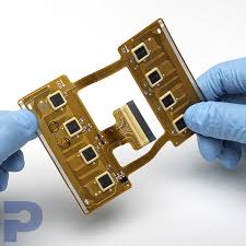
How do you optimize the layout of a flexible PCB?
You can improve the durability of your flex circuit by using a wider trace width, making sure that there are no open joints, and making sure that you use a thinner dielectric material. You can also minimize the number of layers by using a single-sided or double-sided flex PCB. This will reduce the amount of heat that the flex circuit is exposed to and will help it to maintain its elasticity over time.
The material used for a flex PCB is also important to consider, as it will determine how many times your flex circuit can be bent and how flexible it can be. The best material for a flex PCB is polyimide, as it is highly durable and can withstand a range of environmental stresses. Choosing the right materials and components for your PCB can be difficult, but it’s worth the effort to get them right because it will mean that you’ll have a more functional, durable, and reliable electronic product in the end.
Another important aspect to consider when planning a flex PCB is the layer stack and component placement. You can reduce the overall cost of your flex circuit by planning a simple layer stack with minimal holes and cutouts. By doing this, you’ll reduce the number of process units needed for manufacturing, which will save money.
In addition to minimizing the layer count, you can also save money by choosing pad-only plating (button plating). This method allows manufacturers to increase etch yields by reducing the thickness of copper. It also helps the copper bond better to PI substrate and the coverlay, which is beneficial for manufacturability. However, you should keep in mind that button plating is more expensive than standard plated through hole (PTH). This is because it requires additional steps to process the copper.