
Flexible PCBs Perform in High-Flexure
A flex PCB can be used to replace wiring harnesses and ribbon connectors in automotive products and other industrial applications. This allows for lower assembly costs and better design flexibility than traditional wiring harnesses and connectors. Despite this, flexible pcbs have to face certain challenges in high-flexure applications. These include heat, moisture, chemicals, shock & vibration. Understanding these factors helps in designing the right circuit board for the application. This will ensure that the product performs well in harsh environments.
The primary factor that determines a flex PCB’s ability to withstand multiple bending cycles is the thickness of the copper foil used. Thinner copper foil is more pliable and can tolerate higher amounts of flexing than thicker foil. The choice of the copper foil should be determined early on in the design process.
It is also important to decide if the flexible pcbs will be static or dynamic. A static flex PCB will flex only once in its lifetime, while a dynamic flex PCB will flex on a regular basis. Generally, dynamic flex circuits need to have a larger bend radius than static boards.
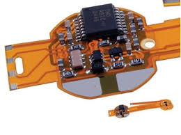
How Flexible PCBs Perform in High-Flexure Applications
In addition to the material selection, the design of the flex PCB has a major impact on its performance. The best way to achieve the required performance is to minimize the number of layers in the flex circuit. This will help to maintain the desired flexing capability and allow for a thinner copper foil, reducing manufacturing cost.
The flex circuit’s copper layer needs to be protected against the elements, which can cause it to oxidize and fail. This can be done with a surface finish, which is available in many different types. One popular option is Electroless Nickel Immersion Gold (ENIG). This is a thin, solderable coating that prevents the copper from oxidizing and protects it against mechanical damage.
To keep traces from breaking when the flex PCB is bent, it is recommended that they be routed perpendicular to the axis that it is being bend or folded along. This will eliminate stress points caused by the traces changing width when the flex circuit is bent, which can lead to cracking and failure of the traces. In cases where the tracing cannot be routed perpendicular to the bend line, a hatched ground should be used.
Another thing to consider when designing a flex PCB is the impedance of the signals. Matching the impedance of the flex circuit to that of the signal source will ensure optimal function and reduce transmission losses. To achieve this, the traces should be designed with a wide end at the connector to allow for an easy solder connection. It is also important to avoid abrupt changes in trace widths. Instead, a gradual transition from the narrow to the wider trace is preferred. This will make the traces more resilient to bending, improving the quality of the connections and extending their lifespan. To accomplish this, pads should be large enough to accommodate the wider traces and pad fillets should be utilized when possible.