
HDI Boards Enable Faster Product Development
As electronics become more compact and powerful, reducing the size of PCBs and the number of layers required to accommodate all necessary features makes it possible to produce smaller devices with greater functionality. However, increasing device complexity requires denser wiring and more advanced components, and conventional PCB constructions can reach their limits. HDI technology offers a solution.
High-density interconnect PCBs use microvias to provide additional connectivity. They offer improved signal strength, reduced weight and lower power consumption while delivering high-reliability and performance. They also feature smaller aspect ratios and faster production times. In addition, their enhanced electrical performance helps reduce problems and speed up troubleshooting.
Several processes and special equipment are needed to manufacture hdi boards, including the laser drilling process that creates the microvias used in the circuit board. These microvias have a diameter less than 150 microns and are used to connect the different layers of the board. They can be stacked or staggered to meet the design goals for each individual layer.
Another critical step in the production process involves etching the copper and pre-preg layers, followed by heat and pressure. Unlike conventional PCBs, HDI boards undergo multiple lamination cycles, which allows the manufacturers to create more complex layers and a wider range of connections.
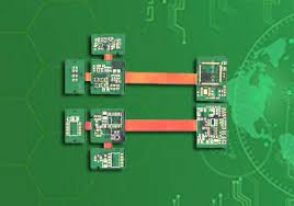
How HDI Boards Enable Faster Product Development
HDI technology can be used in a wide variety of devices, from mobile phones and portable computers to smart weapons and military equipment. They are especially useful in avionics, industrial automation and other fields where devices must communicate with each other. These connections are often necessary for transmitting large amounts of data or ensuring the integrity of critical controls.
In these applications, the increased density of HDI PCBs can create an issue with EMI (electromagnetic interference). The higher levels of connectivity increase the risk of signal interference from adjacent components or from other signals with frequencies that overlap with the intended ones. To avoid this, it is essential to conduct a thorough EMI analysis early in the design process, so any potential issues can be addressed.
It is also essential to have the right CAD tool for designing your HDI circuit board. Look for one that offers features like impedance calculating and automated microvia placement, so you can build the most efficient model possible while staying within your design constraints. It’s also important to prototype your design before committing to full-scale production, so you can catch any errors and test the board under real-world conditions. This will save you the time and expense of reworking your board after the fact. And it can help you bring your product to market more quickly, avoiding expensive delays.
High-Density Interconnect (HDI) PCBs are circuit boards characterized by a higher density of electronic components, smaller traces, and smaller vias than traditional PCBs. These boards utilize microvias, which are significantly smaller than traditional vias, and allow for more densely packed components and shorter signal paths. The increased density and reduced size enable HDI PCBs to support more complex designs with higher performance while maintaining a compact form factor.